The printed circuit board (PCB) is the backbone of most modern electronics, providing the framework to connect components and create functional circuits. Understanding the basics of PCB design, manufacturing, and final artwork preparation is essential for creating reliable and efficient electronic devices. In this guide, we’ll explore the core concepts, from initial design to final artwork, and highlight key considerations for each step in the process.
1. Understanding the Role of a Printed Circuit Board
Printed circuit boards serve as the physical platform for electronic components to connect and function together. A PCB’s design can vary greatly depending on its intended application, from simple single-layer boards to complex multi-layered structures in advanced electronics.
Components and Pathways: PCBs contain conductive pathways, or traces, etched into copper sheets to connect components like resistors, capacitors, and integrated circuits.
Structural Integrity: PCBs use layers of insulating materials like fiberglass to provide rigidity and stability, ensuring the board withstands handling and environmental stress during use.
2. Starting with the PCB Design Process
The PCB design process is where ideas come to life, transforming a circuit diagram into a layout that will be manufactured. A solid design plan ensures that all electrical connections are clear and that components are placed for optimal function and durability.
Choosing the Right Software: PCB design software like Altium Designer, Eagle, and KiCad offer tools to help visualize and organize the layout, schematics, and connections.
Component Placement: Careful placement of components is vital to ensure efficient signal flow, reduce noise, and prevent potential issues with heat dissipation. Designers often arrange components according to a schematic plan, prioritizing critical connections.
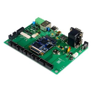
Pressure Sensor Medical Electronic Care Device PCB Board Assembly
3. Creating the Schematic for a PCB
A schematic is a graphical representation of the electrical connections in the circuit. It provides a blueprint for component placement and connections, guiding the design and layout of the PCB.
Symbol and Pin Mapping: Symbols for components and their corresponding pins are defined in the schematic. This mapping helps designers connect components accurately during the layout process.
Netlist Generation: The netlist, derived from the schematic, lists all connections and forms the basis for routing paths on the PCB layout. Any errors in the schematic or netlist can lead to functionality issues in the final product.
4. Designing the PCB Layout
The layout design translates the schematic into a physical arrangement that defines where each component and pathway will be placed on the board. This step requires precision and attention to detail, as it will directly impact the board’s performance.
Layer Configuration: Simple circuits may use a single layer, while more complex designs require multiple layers. Multi-layer PCBs offer more flexibility and reduce interference between circuits.
Routing Paths: Routing paths connect the pins of each component based on the netlist. Automated routing tools can help streamline this process, although manual adjustments are often needed for optimization.
5. Adding Power Planes and Ground Layers
In multi-layer PCBs, power planes and ground layers help improve the stability of the power supply, reduce electromagnetic interference (EMI), and minimize resistance. Proper configuration of these layers is essential for a stable circuit.
Power and Ground Optimization: Placing power and ground layers directly next to each other reduces loop inductance and ensures efficient current flow.
Noise Reduction: Strategic placement of ground planes helps in reducing noise and improves signal integrity, particularly in high-speed circuits.
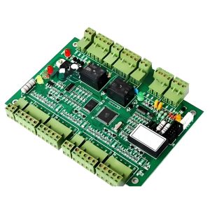
Electronic Copying PCB Manufacturing Assembly Design
6. Preparing the Final Artwork
After finalizing the PCB layout, the design is prepared as a set of “artwork” files that will guide the manufacturing process. These files, usually in Gerber format, include all the details required to etch copper paths, drill holes, and add component markings.
Generating Gerber Files: Gerber files contain information for each layer of the PCB, including copper layers, solder mask, and silkscreen layers. They are essential for precise manufacturing, ensuring each feature is accurately rendered.
Drill Files and Assembly Drawings: Drill files specify the locations and sizes of holes needed for components and mounting, while assembly drawings assist with component placement during assembly.
7. Conducting a Design Rule Check (DRC)
Before sending files to manufacturing, designers run a Design Rule Check (DRC) to ensure compliance with all layout rules and identify potential issues. The DRC verifies trace width, spacing, and clearance, helping avoid manufacturing errors and ensuring functionality.
Error Prevention: The DRC catches issues that could cause short circuits, interference, or production failures, allowing designers to make adjustments before finalizing.
Improved Reliability: By ensuring design rules are met, the DRC helps improve the reliability and performance of the final PCB.
Questions and Answers About PCB Basics
Q1: What materials are commonly used in PCBs?
A1: Most PCBs are made with layers of fiberglass for strength, with copper layers etched to create electrical paths. For flexible applications, polyimide materials may be used.
Q2: Why are multi-layer PCBs used?
A2: Multi-layer PCBs allow for complex routing, minimizing interference and improving performance in high-speed or densely packed circuits.
Q3: What is the role of Gerber files in PCB manufacturing?
A3: Gerber files contain detailed instructions for each layer of the PCB, guiding the manufacturing process to ensure each element, from copper traces to drill holes, is accurately created.
From initial design and layout to preparing the final artwork, each stage in PCB development is critical for creating a high-quality product. With attention to detail and a focus on precision, you can produce reliable, efficient PCBs for any electronic application.
For more information or assistance in finding the a professional PCB and PCBA assembly manufacturer, contact Thriver Digita. Thriver Digita provides OEM/ODM PCBA,One stop service from PCB Design,PCB Copy,BOM Kitting,Components Sourcing, PCB Manufacturer, PCB Assembly,Function Testing,etc.


